The ACIS instrument team is in the middle of an ambitious calibration program at the writing of this article. Well over a hundred CCDs have been produced at MIT Lincoln Laboratories (LL), from which ten will be selected for the flight focal plane and ten for the backup focal plane. The ACIS subassembly calibration consists of several, mostly independent, activities, requiring measurements in the ACIS team's own laboratories at MIT and Penn State and at national and international synchrotron facilities. These activities include the calibration of flight-quality CCDs at the BESSY synchrotron to be used as transfer-standards against the flight CCDs, the screening of the flight candidate CCDs in order to identify the best candidates, the detailed calibration of the X-ray performance of the flight CCDs, the calibration of the optical blocking filters at the Wisconsin and Brookhaven synchrotrons, and the integrated test of the flight instrument at MIT LL. This effort began in earnest in 1995 and will continue into 1997, culminating with the calibration of ACIS with the HRMA and gratings at the XRCF.
The expected calibration accuracies will far exceed any
previously attained in X-ray astronomy; for example, the goal for
detection efficiency accuracy is 1% on ![]() pixel regions
and the goal for the energy scale calibration is 0.1%
(Bautz, et al. 1996, SPIE). In order to
achieve these levels of
accuracy, the ACIS team has developed a multi-phase calibration plan
to provide the necessary data over the 0.1-10.0 keV band.
The different phases of the subassembly calibration will be outlined
in the sections
below. More detailed information about each of these phases can be
found in the papers written by the ACIS team and referenced below.
The MIT papers will be accessible from the
MIT CCD group home page
and the Penn State papers are
currently available on the WWW.
An overview of the calibration objectives can be found in an ACIS team
memo entitled
ACIS CCD Subassembly Calibration Plan.
pixel regions
and the goal for the energy scale calibration is 0.1%
(Bautz, et al. 1996, SPIE). In order to
achieve these levels of
accuracy, the ACIS team has developed a multi-phase calibration plan
to provide the necessary data over the 0.1-10.0 keV band.
The different phases of the subassembly calibration will be outlined
in the sections
below. More detailed information about each of these phases can be
found in the papers written by the ACIS team and referenced below.
The MIT papers will be accessible from the
MIT CCD group home page
and the Penn State papers are
currently available on the WWW.
An overview of the calibration objectives can be found in an ACIS team
memo entitled
ACIS CCD Subassembly Calibration Plan.
Note: The Web Page containing this document at MIT has been removed.
The first task in this process is to identify CCDs which pass the
selection criteria for flight-candidate CCDs. MIT LL performs
several tests on the CCDs before they leave the fabrication
facility.
These tests check the functionality of the 4 quadrants and output
nodes, the gain, the noise, the dark current, and for the existence of
bad columns and hot pixels at a temperature of -40 C.
If the CCD passes all of these
tests, it is sent to the MIT Center for Space Research (CSR) where a
more detailed screening of the X-ray performance is acquired.
The first order of business is to determine the
optimal clocking voltages, which provide the lowest noise and a
reasonable gain, at a temperature of -120 C. The CCDs are exposed to
an Fe55 source (5.898 keV) for these measurements and are then later
exposed to
![]() 1.485 keV X-rays. All three data
sets are used
to measure the charge-transfer inefficiency (CTI), readout noise,
spectral resolution and detection uniformity of the CCD. In addition
to these data, measurements are made at several exposure times to
determine the dark current. And of course, these data are used to
identify any new bad columns or hot pixels. These procedures, the
selection criteria and
preliminary results are described in more detail in Pivovaroff, et al.
1996. Flight-candidate CCDs will typically have a RMS readout
noise of 2-4
1.485 keV X-rays. All three data
sets are used
to measure the charge-transfer inefficiency (CTI), readout noise,
spectral resolution and detection uniformity of the CCD. In addition
to these data, measurements are made at several exposure times to
determine the dark current. And of course, these data are used to
identify any new bad columns or hot pixels. These procedures, the
selection criteria and
preliminary results are described in more detail in Pivovaroff, et al.
1996. Flight-candidate CCDs will typically have a RMS readout
noise of 2-4 ![]() , CTI below
, CTI below ![]() , and spectral
resolution within 10% of the theoretical limit. More than 30
CCDs have been measured which pass the selection criteria.
, and spectral
resolution within 10% of the theoretical limit. More than 30
CCDs have been measured which pass the selection criteria.
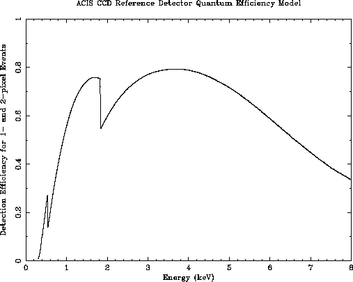
Figure 3: The model detection efficiency for 1 and 2 pixel events as a
function of energy for a front-illuminated CCD (from Bautz, et al. 1996).
The ACIS team has been conducting measurements at the Berliner Elektron Speicherring Synchrotron (BESSY) with flight-quality CCDs in order to calibrate the absolute detection efficiency. The BESSY synchrotron provides undispersed radiation in the 0.1-10.0 keV band which is calculable to better than 1% accuracy. Several trips have been made in 1995 and 1996 with several different CCDs. In addition, monochromators at BESSY have been used to characterize the CCD response near absorption edges where the response of the device is changing rapidly with energy. These CCDs are then returned to the MIT laboratory where they are used as transfer-standard reference detectors. Therefore, the BESSY data provide the foundation on which the absolute calibration rests for the flight CCDs.
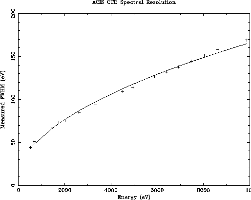
Figure 4: The measured spectral resolution for 1 and 2 pixel
events as a function of energy for a front-illuminated CCD (from
Bautz, et al. 1996). The data were fit with a single gaussian at each
energy. The error bars of ![]() eV represent the repeatibility of
the measurements. The fitted readout noise is
eV represent the repeatibility of
the measurements. The fitted readout noise is ![]() and the
fitted value for the fano factor F times the mean ionization
potential per electron-hole pair
and the
fitted value for the fano factor F times the mean ionization
potential per electron-hole pair ![]() is
is ![]() .
.
The ACIS team has developed five laboratory setups (two of which are
identical and redundant), each with a specific calibration goal in mind. A
grating spectrometer has been developed to measure the spectral
response of the CCDs over the 0.2-1.5 keV range (Prigozhin, et al. 1996),
with a special emphasis on the study of the O-K edge ( ![]() eV).
Another spectrometer has been developed to scan the Si-K edge
(
eV).
Another spectrometer has been developed to scan the Si-K edge
( ![]() eV).
A third spectrometer is used to collect the screening data discussed
above. The last (twin) setup collects the majority of the
subassembly data since it is the chamber which houses both a test CCD
and a BESSY-calibrated reference CCD (Jones, et al. 1996), hence the
advantage of having two setups. This chamber produces both
spectral resolution measurements at 16 energies and quantum
efficiency measurements at 8 energies. The chamber contains
Tritium-fluoresced C, O, and F sources and Al, Si, P, Cl, Ti, V, Mn, Fe,
Co, Zn, Ge, & Ni targets fluoresced by a Molybdenum target excited
by a 15 keV electron beam. This chamber also contains an Fe55 source.
For the quantum efficiency measurements,
eV).
A third spectrometer is used to collect the screening data discussed
above. The last (twin) setup collects the majority of the
subassembly data since it is the chamber which houses both a test CCD
and a BESSY-calibrated reference CCD (Jones, et al. 1996), hence the
advantage of having two setups. This chamber produces both
spectral resolution measurements at 16 energies and quantum
efficiency measurements at 8 energies. The chamber contains
Tritium-fluoresced C, O, and F sources and Al, Si, P, Cl, Ti, V, Mn, Fe,
Co, Zn, Ge, & Ni targets fluoresced by a Molybdenum target excited
by a 15 keV electron beam. This chamber also contains an Fe55 source.
For the quantum efficiency measurements, ![]() counts are
collected at each energy over the entire CCD; for the spectral
resolution measurements,
counts are
collected at each energy over the entire CCD; for the spectral
resolution measurements, ![]() counts are collected at each energy.
In addition to being measured against the reference CCDs, the flight CCDs
are also measured against a Si(Li) detector (Manning, et al. 1996).
Figure 3 shows a preliminary QE curve derived from these data,
accepting single and two pixel events, for a
front-illuminated CCD which is typical of the flight-candidate CCDs.
The high energy QE is dramatically higher if the event
selection is changed to include 3 and 4 pixel events.
Figure 4 shows the spectral resolution measurements for the same CCD,
also selecting 1 and 2 pixel events.
counts are collected at each energy.
In addition to being measured against the reference CCDs, the flight CCDs
are also measured against a Si(Li) detector (Manning, et al. 1996).
Figure 3 shows a preliminary QE curve derived from these data,
accepting single and two pixel events, for a
front-illuminated CCD which is typical of the flight-candidate CCDs.
The high energy QE is dramatically higher if the event
selection is changed to include 3 and 4 pixel events.
Figure 4 shows the spectral resolution measurements for the same CCD,
also selecting 1 and 2 pixel events.
Three main types of measurements are performed on the flight-candidate
filters: spatial uniformity measurements, detailed scans around
absorption edges, and optical light rejection efficiency. The spatial
uniformity measurements are
performed at the University of Wisconsin Synchrotron Radiation Center
(SRC) at energies of 273, 522, 775, 1330, and 1860 eV
(Townsley, et al. 1996). The spatial uniformity is measured on a 0.75 mm
scale which matches the ![]() pixel scale on which the CCD QE is
measured. Preliminary measurements have identified non-uniformities
varying from 0.5% to 2.0%. The transmission of the filters around
important edges is measured at the National Synchrotron Light Source
at Brookhaven National Laboratory (Chartas, et al. 1996). The C, Ni, O,
Al, and Si edge
regions are scanned using a spectrometer/reflectometer which can
provide resolution better than 0.1 eV. These data have revealed the
extended X-ray absorption fine structure (EXAFS) near absorption
edges. Finally, the filters are
exposed to diffuse optical light to search for pinholes and leaks in a
laboratory setup at Penn State.
pixel scale on which the CCD QE is
measured. Preliminary measurements have identified non-uniformities
varying from 0.5% to 2.0%. The transmission of the filters around
important edges is measured at the National Synchrotron Light Source
at Brookhaven National Laboratory (Chartas, et al. 1996). The C, Ni, O,
Al, and Si edge
regions are scanned using a spectrometer/reflectometer which can
provide resolution better than 0.1 eV. These data have revealed the
extended X-ray absorption fine structure (EXAFS) near absorption
edges. Finally, the filters are
exposed to diffuse optical light to search for pinholes and leaks in a
laboratory setup at Penn State.
Bautz, M, ``ACIS Subassembly Calibration Plan'', 1996 ACIS Team Memo,
Bautz, M., Kissel, S., Prigozhin, G., Jones, S., Isobe, T., Manning, H., Pivovaroff. M., Ricker, G., & Woo, J., ``X-ray Calibration for the AXAF CCD Imaging Spectrometer'', 1996 SPIE 2805
Chartas, G., Garmire, G., Nousek, J., & Townsley, L., ``ACIS UV/Optical Blocking Filter Calibration at the National Synchrotron Light Source'', 1996 SPIE 2805,
Jones, S.E., Bautz, M.W., Kissel, S., & Pivovaroff. M., G.R., ``Using Tritium and X-ray Tubes as X-ray Calibration Sources for ACIS'', 1996 SPIE 2805
Manning, H.L., Jones, S.E., Kissel, S.E., Bautz, M.W., & Ricker, G.R., ``Quantum Efficiency Calibration of AXAF CCDs from 2-10 keV'', 1996 SPIE 2805
Pivovaroff. M., Kissel, S., Bautz, M.W., Prigozhin, G., Isobe, T., Woo, J. & Gregory, J.A., ``Flight X-ray CCD Selection for ACIS'', 1996 SPIE 2805
Prigozhin, G., Bautz, M.W., Gendreau, K., & Ricker, G., ``Calibration of X-ray CCDs with an Erect Field Grating Spectrometer in the 0.2-1.5 keV Band'', 1996 SPIE 2805
Townsley, L., Powell, F.R., MacKay, J.F., Lagally, M.G., Nousek, J., & Garmire, G., ``Transmission Maps of the ACIS UV/Optical Blocking Filters'', 1996 SPIE 2805,
Paul Plucinsky