AXAF has seen the future in the application of charge-coupled devices (CCDs) to X-ray astronomy. Its gaze is fixed resolutely...backward?
Well, yes, in a manner of speaking: two of the ten detectors in the AXAF CCD Imaging Spectrometer (ACIS) are backside-illuminated CCDs. These detectors, which (like all of the ACIS CCDs) have been manufactured by MIT's Lincoln Laboratories, will substantially boost the sensitivity of ACIS to soft X-rays. As a result, ACIS will be more efficient, and its powerful combination of spatial and spectral resolution can be brought to bear on fainter and/or softer sources than if ACIS were populated only with ``conventional,'' frontside-illuminated CCDs. At the same time, the new breed of backside-illuminated detector brings with it a host of new calibration problems and challenges; the ASC and the ACIS team are grappling with these issues as analysis of ACIS calibration data proceeds.
A conventional CCD consists of a sandwich of semiconductor layers overlaid
with a network of ``gates,'' electrodes which serve to transfer charge from
one pixel to another as the device is read out. At low energies ( ![]() keV) the presence of these gates makes it difficult for photons to penetrate
to the semiconductor layers, where they can liberate electrons and thereby
be detected. Thus the gates reduce the sensitivity of conventional CCDs to
soft X-rays. Backside-illuminated CCDs are, as the name suggests, CCDs
which are ``flipped'' with respect to the direction of incoming photons.
Since they are upside-down, they enjoy a ``gateless'' view of incoming
radiation. In addition, the semiconductor wafers used in
backside-illuminated devices are ``thinned'' during fabrication; whereas the
thickness of frontside-illuminated CCDs is typically ~500µm ,
backside-illuminated devices are whittled down to a mere 45 µm. This
enhances the likelihood that the charge released near the back of a
backside-illuminated CCD by an incident low-energy photon will be fully
collected by the gates at the front of the device. The net result is
significantly higher quantum efficiency at low energies (see Figure 13).
keV) the presence of these gates makes it difficult for photons to penetrate
to the semiconductor layers, where they can liberate electrons and thereby
be detected. Thus the gates reduce the sensitivity of conventional CCDs to
soft X-rays. Backside-illuminated CCDs are, as the name suggests, CCDs
which are ``flipped'' with respect to the direction of incoming photons.
Since they are upside-down, they enjoy a ``gateless'' view of incoming
radiation. In addition, the semiconductor wafers used in
backside-illuminated devices are ``thinned'' during fabrication; whereas the
thickness of frontside-illuminated CCDs is typically ~500µm ,
backside-illuminated devices are whittled down to a mere 45 µm. This
enhances the likelihood that the charge released near the back of a
backside-illuminated CCD by an incident low-energy photon will be fully
collected by the gates at the front of the device. The net result is
significantly higher quantum efficiency at low energies (see Figure 13).
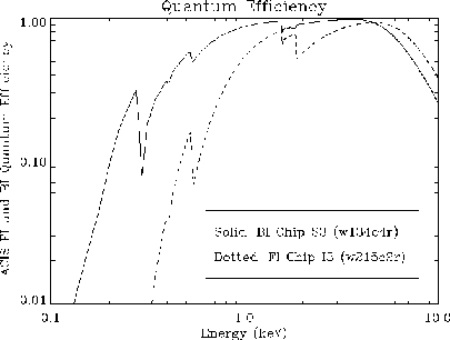
Figure 13: Comparison of QE of front- and back-illuminated CCDs.
The lack of gate
structure at the exposed surface of the back-illuminated device, combined
with its reduced physical thickness, results in improved QE for
energies
![]() keV; the improvement is most substantial (more than a factor 3) for
incident photon energies
keV; the improvement is most substantial (more than a factor 3) for
incident photon energies ![]() keV. Note the decreased QE of the
back-illuminated CCD relative to that of the front-illuminated CCD at high
energy (
keV. Note the decreased QE of the
back-illuminated CCD relative to that of the front-illuminated CCD at high
energy ( ![]() keV), due to photon loss through the front of the
back-illuminated device. Source: Proposer's Guide. Postscript version of the above image.
keV), due to photon loss through the front of the
back-illuminated device. Source: Proposer's Guide. Postscript version of the above image.
The potential benefits to AXAF of an ACIS that sports a combination of frontside- and backside-illuminated CCDs are manifold, in both the imaging and spectroscopy realms. The superior spectral resolution, comparative ease in calibration, and proven track record of frontside-illuminated devices make them essential components of ACIS; while the inclusion of backside-illuminated devices, with their superior low-E quantum efficiency, at certain key positions in the spectroscopic (ACIS-S) CCD array will produce higher photon detection rates for most X-ray sources. Particular types of AXAF programs that stand to benefit from the introduction of backside-illuminated CCDs include (but are certainly not limited to):
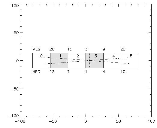
Figure 14: Layout of ACIS-S array showing
placement of backside-illuminated CCDs as the shaded chips. The six chips
are numbered in the upper left corner of each.
The location of the HEG (dashed line) and the
MEG (dot-dash line) spectra are shown.
The vertical line intersects the spectra at the aim point.
The approximate wavelengths (in Å)
of the chip boundaries is given for the MEG above the array and
for the HEG below the array. Axes are in mm.
In cutting-edge instrumentation there is seldom a free lunch, of course. The increased low-E QE of backside-illuminated CCDs -- with its potential improvement in AXAF's capabilities -- will come at the cost of certain degradations in CCD performance, not to mention sheer sweat and toil in understanding and calibrating the new devices. Back-illuminated devices have relatively poor charge transfer efficiency compared with the frontside-illuminated CCDs in ACIS; prior to radiation exposure, the Lincoln Labs frontside-illuminated devices essentially perform flawlessly as they pass charge from pixel to pixel during readout. In addition, charge liberated by a low-energy photon is spread over more pixels when the photon is detected by a back-illuminated device, increasing the chances that freed electrons will go uncounted. This loss of charge during photon detection and subsequent pixel readout translates into degraded spectral resolution, as well as significant gain non-linearity. Also, the backside-illuminated devices have more bad columns and bad pixels than the (nearly defect-free) frontside-illuminated devices.
Perhaps most importantly, there is no base of long-term experience on which to judge the reliability of backside-illuminated CCDs. Unlike frontside-illuminated devices, which have a proven track record derived from years of rigorous lab tests and more than four years of data-taking aboard ASCA, backside-illuminated CCDs have only recently come under close scrutiny in the lab. Nevertheless, the potential science benefit offered by a ``mixed'' array of frontside- and backside-illuminated devices led the AXAF project to take the calculated risk, and fly both flavors of CCD.
After last year's spirited debate involving many sectors of the AXAF
community, the SWG and IPIs reached consensus on the placement of the
backside-illuminated devices in the ACIS-S (as opposed to the imaging
ACIS-I) array. ACIS-S consists of 6 CCDs that follow the focal surface of
the dispersive HETG (Figure 14).
However, CCD S-3 offers the best
imaging performance of any single CCD on ACIS, since its center lies closer
to the telescope boresight, and it is more nearly orthogonal to the
telescope optical axis, than any other ACIS CCD
(the CCDs in ACIS-I are tilted to optimize image quality over their entire
2x2 CCD field of view). As a result, S-3 will offer imaging at 2'' or
better resolution over essentially all of its 8' square field of view.
Since S-3 is expected to be an imaging workhorse, the SWG and IPIs decided
to place the best available backside-illuminated device at this position. A
second backside-illuminated CCD has been placed on the opposite side of
the spectroscopy array, at position S-1.
The presence of a back-illuminated CCD at this position will
increase the effective area of the HETG/ACIS-S combination, particularly
over the wavelength range from ![]() 15 Åto 26 Å(i.e., for the MEG
spectrum; see Figures).
The presence of front-illuminated
CCD's at positions S-4 and S-5 then provides HETG with a complementary
``conventional" detector on the opposite side
of the ACIS-S array.
15 Åto 26 Å(i.e., for the MEG
spectrum; see Figures).
The presence of front-illuminated
CCD's at positions S-4 and S-5 then provides HETG with a complementary
``conventional" detector on the opposite side
of the ACIS-S array.
Only time (and hard calibration work) will tell if the project's confidence in backside-illuminated devices is borne out by a more scientifically fruitful AXAF. Whatever the outcome, the inclusion of the new backward-facing CCDs in ACIS represents a daring step -- forward -- for X-ray astronomy.
Joel H. Kastner